 Code:
DE09 Subject:
DIGITAL ELECTRONICS
Code:
DE09 Subject:
DIGITAL ELECTRONICS
Time: 3 Hours Max. Marks: 100
NOTE: There are 9 Questions in all.
· Question 1 is compulsory and carries 20 marks. Answer to Q. 1. must be written in the space provided for it in the answer book supplied and nowhere else.
· Out of the remaining EIGHT Questions answer any FIVE Questions. Each question carries 16 marks.
· Any required data not explicitly given, may be suitably assumed and stated.
Q.1 Choose the correct or best alternative in the following: (2x10)
a. The result of adding hexadecimal number A6 to 3A is
(A) DD. (B) E0.
(C) F0. (D) EF.
b. A universal logic gate is one, which can be used to generate any logic function. Which of the following is a universal logic gate?
(A) OR (B) AND
(C) XOR (D) NAND
c. The logic 0 level of a CMOS logic device is approximately
(A) 1.2 volts (B) 0.4 volts
(C) 5 volts (D) 0 volts
d. Karnaugh map is used for the purpose of
(A) reducing the electronic circuits used.
(B) to map the given Boolean logic function.
(C) to minimize the terms in a Boolean expression.
(D) to maximize the terms of a given a Boolean expression.
e. A full adder logic circuit will have
(A) two inputs and one output.
(B) three inputs and three outputs.
(C) two inputs and two outputs.
(D) three inputs and two outputs.
f. An eight stage ripple counter uses a flipflop with propagation delay of 75 nanoseconds. The pulse width of the strobe is 50ns. The frequency of the input signal which can be used for proper operation of the counter is approximately
(A) 1 MHz. (B) 500 MHz.
(C) 2 MHz. (D) 4 MHz.
g. The output of a JK flipflop with asynchronous preset and clear inputs is ‘1’. The output can be changed to ‘0’ with one of the following conditions.
(A) By applying J = 0, K = 0 and using a clock.
(B) By applying J = 1, K = 0 and using the clock.
(C) By applying J = 1, K = 1 and using the clock.
(D) By applying a synchronous preset input.
h. The information in ROM is stored
(A) By the user any number of times.
(B) By the manufacturer during fabrication of the device.
(C) By the user using ultraviolet light.
(D) By the user once and only once.
i. The conversation speed of an analog to digital converter is maximum with the following technique.
(A) Dual slope AD converter.
(B) Serial comparator AD converter.
(C) Successive approximation AD converter.
(D) Parallel comparator AD converter.
j. A weighted resistor digital to analog converter using N bits requires a total of
(A) N precision resistors. (B) 2N precision resistors.
(C) N + 1 precision resistors. (D) N – 1 precision resistors.
Answer any FIVE Questions out of EIGHT Questions.
Each question carries 16 marks.
Q.2 a. Give the details of excess 3 code and gray code using four binary digits. Compare the two codes. (8)
b. Convert the decimal number 45678 to its hexadecimal equivalent number. (4)
c. Write the truth table of NOR gate. (4)
Q.3 a. Distinguish between enhancement mode and depletion mode metal oxide semiconductor field effect transistors giving their characteristics. (6)
b. List out the characteristics of digital integrated circuits which are used to compare their performances. Briefly explain each one of them. (6)
c. Explain the purpose served by using don’t care condition in the simplification of Boolean expressions using a Karnaugh map. (4)
Q.4 a. Draw the circuits of a CMOS inverter and explain its operation. (4)
b. Design a BCD to excess 3 code converter using minimum number of NAND gates. Hint: use k map techniques. (8)
c. What do you understand by tri-state logic gates? Explain the functioning of a tri-state NAND gate. (4)
Q.5 a. Design a 4 : 1 multiplexer with strobe input using NAND gates. (5)
b. Draw the circuit diagram of a BCD adder and explain the logic behind the circuit. (5)
c. Draw the block diagram of a BCD to seven segment decoder/driver for one BCD digit. Explain the relation between BCD input and seven segments. (6)
Q.6 a. Draw the circuit and explain the working of a JK flipflop using NAND gates with asynchronous ‘clear’ and ‘set’ inputs. (8)
b. Explain what do you understand by race-around condition. (4)
c. With the help of a suitable diagram, explain how do you convert a JK flipflop to T type flipflop. (4)
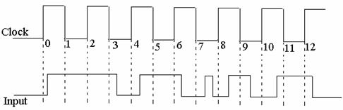
Q.7 a. The clock and the input waveforms shown below are applied to the D input of a positive edge triggered D flipflop. Sketch the output waveforms. (6)
b. Design a 3 bit binary up/down counter with a direction control M using JK flipflops. Show the details of K maps. (10)
|
Q.8 a. A number of 256 x 8 bit memory chips are available. Design a memory organization to create a 2 K x 8 memory. Identify the requirements of 256 x 8 memory chips and explain the details. (8)
b. What are the specifications/ characteristics used by the manufacturers to describe a digital to analog converter. Explain each one briefly. (8)
Q.9 a. Draw and explain the function of dual slope analog to digital converter. Derive the equations used. (8)
b. Draw a R-2R ladder digital to analog converter using 8 bit input and explain its operation. If the reference voltage is 5 volts. Calculate the output if the input code is 0 1 0 1 0 1 0 1. (8)