 Code: DC02 Subject:
FUNDAMENTALS OF ELECTRONICS
Code: DC02 Subject:
FUNDAMENTALS OF ELECTRONICS
Time: 3 Hours Max. Marks: 100
NOTE: There are 9 Questions in all.
· Question 1 is compulsory and carries 20 marks. Answer to Q. 1. MUST BE WRITTEN IN THE SPACE PROVIDED FOR IT in the answer book supplied and nowhere else.
· Out of the remaining EIGHT Questions answer any FIVE Questions. Each question carries 16 marks.
· Any required data not explicitly given, may be suitably assumed and stated.
Q.1 Choose the correct or best alternative in the following: (2x10)
a. A resistor has a colour band sequence: yellow, violet, orange, and gold. Its value is
(A)
![]()
![]() 5% (B)
5% (B)
![]()
![]() 5%
5%
(C)
![]()
![]() 5%. (D)
5%. (D)
![]()
![]() 5%
5%
b. The resistance of a voltage source is of strength 20V is 100![]() . Its equivalent
current source is
. Its equivalent
current source is
(A)
a source
of strength 20A in shunt with a resistance of 100![]()
(B)
a source
of strength 0.3A in shunt with a resistance of 100![]()
(C)
a
source of strength 0.2A in shunt with a resistance of 100![]()
(D)
a
source of strength 2A in shunt with a resistance of 100![]()
c. In almost all applications, vaccum tubes have been replaced by solid-state devices. But the vaccum tubes are still in use where
(A) very long life of the device is a necessary requirement
(B) very low-frequency signals are involved
(C) very high power is to be handled
(D) portability of the electronic system is an important factor
d. If in the forward characteristic of a PN-junction diode, a voltage change of 0.07V around the operating point results in a current change of 7.5mA, then the dynamic resistance of the diode is
(A)
8.52 K![]() (B)
8.92
(B)
8.92 ![]()
(C) 5.3 K![]() (D)
9.46
(D)
9.46 ![]()
e. A LED emits visible light when its
(A) PN-junction is reversebiased (B) holes and electrons recombine
(C) depletion region widens (D) PN-junction becomes hot
f. In the logic circuit shown, the Boolean expression for the output X is
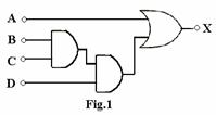
(A)
![]()
(B) A+BCD
(C) AB+D
(D) BC+AD
g. CMOS circuits are extensively used for on-chip computers mainly because of their extremely
(A) low power consumption (B) large packing density
(C) high noise immunity (D) low cost
h. The foundation on which an IC is built is called a/an
(A) insulator (B) wafer
(C) base (D) plate
i. Monolithic IC construction uses
(A) Discrete components (B) high value resistors
(C) connecting wires (D) extensive number of components
j A sinusoidal voltage
of peak value 5 mV and frequency one kilohertz is applied to an OPAMP differentiator
circuit. If the values of the resistor and the capacitor used in the circuit
are 1000K![]() and 1μF, respectively, then the peak value of the output voltage will be
around
and 1μF, respectively, then the peak value of the output voltage will be
around
(A) 2200mV (B) 3140mV
(C) 225mV (D) 1032mV
Answer any FIVE Questions out of EIGHT Questions.
Each question carries 16 marks.
Q.2 a. Which are the basic components used in all electronic circuits? (5)
b. Write a brief notes on the following
(i) Filter chokes, (ii) Audio-frequency chokes (7)
c. A
600![]() , 2V
a.c. source is connected to a variable load, ZL. The load can vary
from 50K
, 2V
a.c. source is connected to a variable load, ZL. The load can vary
from 50K![]() to 500K
to 500K![]() .
Find the variation in the terminal voltage of the source (4)
.
Find the variation in the terminal voltage of the source (4)
Q.3 a. Distinguish between an intrinsic semiconductor and an extrinsic semi-conductor. Explain briefly the effect of temperature on the conductivity of intrinsic semiconductors. (7)
b. What is the most important characteristic of a PN-junction? Give the meaning of the following as applied to a P-N junction:
(i) Forward bias & reverse bias
(ii) Depletion region
(iii) Cut-in voltage
(iv) Breakdown voltage (9)
Q.4 a. Distinguish between power diodes and zener diodes. (11)
b. What is a Schottky diode? Where is it mainly used? Illustrate the scheme and circuit symbol of a Schottky diode by figures. (5)
Q.5 a. What is a junction transistor? Briefly explain the structure of a junction transistor. (8)
b. A transistor has a dc alpha of 0.98 and collector leakage current of one microampere. For an emitter current of 2mA, evaluate the collector current and the base current for the transmitter. (4)
c. For an N-channel JFET,IDSS=8.7mA, VP= –3V, VGS= –1V. Calculate the values of ID and gmo. (4)
Q.6 a. Draw the circuit of a voltage divider bias for a BJT and mention its features.
A voltage divider bias circuit uses a PNP transistor
with β=60. The collector resistance and the emitter resistance are 5K![]() and 1K
and 1K![]() respectively. If
the voltage-divider is comprised of 40K
respectively. If
the voltage-divider is comprised of 40K![]() and 5K
and 5K![]() resistors, calculate the dc bias
voltages and the currents for the circuit if
resistors, calculate the dc bias
voltages and the currents for the circuit if
VCC = 12V. Take VBE = 0.3V. (12)
b. A Hartley oscillator uses two inductors of value 0.1mH and 10μH, respectively. If the mutual inductance between the coils used is 20μH, calculate the value of the capacitor required for the oscillator circuit to obtain an output frequency of 4110 KHz. (4)
Q.7 a.
Prove the following using the basic laws and postulates of Boolean algebra: (i)
![]()
(ii) X + XY = X
Indicate the postulates used in each step of your proof. (6)
b. For the given Karnaugh map, write the decimal representation of the maxterm canonical expression. (3)
|
|
YZ |
|
|
|
|
X |
1 |
0 |
0 |
1 |
|
|
1 |
1 |
0 |
0 |

Fig.2
c. Using a Karnaugh map, determine the minimal sum for the Boolean function given below
![]() (7)
(7)
Q.8 a. Comment on the flexibilities available in different IC logic families, which must be considered while selecting a logic family for a particular job. (5)
b. Draw the circuit of a TTL gate with totem-pole output driver and briefly explain. Why are clamping diodes commonly used in all TTL gates? (11)
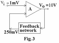
Q.9 a. What is a feedback amplifier? In the feedback amplifier scheme shown in figure determine the gain of the feedback circuit and the gain of the amplifier with feed back. (6)
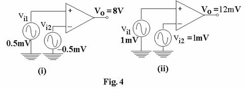
b. For the circuit measurements shown in the figure, calculate CMRR is decibels. (6)
c. Write a note on “capacitor in monolithic circuits”. (4)