Code: AE09 Subject: ANALOG & DIGITAL ELECTRONICS
 Time:
3
Hours
Max. Marks: 100
Time:
3
Hours
Max. Marks: 100
NOTE: There are 9 Questions in all.
· Question 1 is compulsory and carries 20 marks. Answer to Q. 1. must be written in the space provided for it in the answer book supplied and nowhere else.
· Out of the remaining EIGHT Questions answer any FIVE Questions. Each question carries 16 marks.
· Any required data not explicitly given, may be suitably assumed and stated.
Q.1 A. Choose the correct or best alternative in the following: (2x10)
a. A typical value of the output resistance at room temperature for the 741 OPAMP is
(A)
![]() . (B)
. (B)
![]() .
.
(C)
![]() . (D)
. (D)
![]() .
.
b. If the OPAMP specifications lists the input offset voltage as 1.2 mV, then for the circuit shown in Fig.1, the output offset voltage is
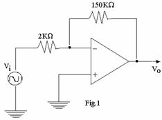
(A) 81.2 mV.
(B) 72.2 mV.
(C) 91.2 mV.
(D) 90 V.
c. In a first-order
high-pass active filter, if the values of the resistance and the capacitance
used are 2.1 ![]() and
and
![]() respectively,
then the cut-off frequency of the filter is equal to
respectively,
then the cut-off frequency of the filter is equal to
(A) 15 KHz. (B) 1.5 KHz.
(C) 3.5 KHz. (D) 0.95 KHz
d. For a counter-type ADC, if the conversion time is around 4.1 ms then the minimum number of conversions that could be carried out each second would be approximately
(A) 150 per second. (B) 244 per second.
(C) 90 per second. (D) 209 per second.
e. Typical propagation delay of a CMOS gate ranges from
(A) 2 to 15 ns. (B) 25 to 150 ns.
(C) 100 to 200 ns. (D) 80 to 120 ns.
f. The number of
address bits needed to operate a 2K ![]() 8-bit RAM are:
8-bit RAM are:
(A) 9 (B) 25
(C) 15 (D) 11
g. A one-to-sixteen demultiplexer requires
(A) 2 select input lines. (B) 3 select input lines.
(C) 8 select input lines. (D) 4 select input lines.
h. The charge coupled devices are implemented using
(A) CMOS Technology (B) PMOS Technology
(C) MOS Technology (D) NMOS Technology
i. Schottky diodes exhibit a storage time of approximately
(A) Zero sec. (B) 20 sec.
(C) 30 ns. (D) 32 ms.
j. In an analog multiplier, if both the inputs are positive or negative then the multiplier is said to be
(A) a two quadrant multiplier. (B) a one quadrant multiplier.
(C) a four quadrant multiplier. (D) a three quadrant multiplier.
Answer any FIVE Questions out of EIGHT Questions.
Each question carries 16 marks.
Q.2 a. What is an OPAMP? What do you mean by common mode operation? What will be the output voltage for the above operation, ideally? (4)
b. Briefly explain how the following can be measured for an OPAMP:
(i) Input offset voltage ![]() (ii)
Bias current
(ii)
Bias current ![]()
(iii)
Input offset current ![]() (9)
(9)
c. Determine the cutoff frequency of an OPAMP, whose dc gain is
200 V/mV and unity gain bandwidth is one megahertz. (3)
Q.3 a. What is an active filter? Define an ideal band-pass filter and illustrate its response characteristic. Can active filters be designed up to frequencies of several MHz? Justify your answer. (6)
b. Design a first order low-pass active filter to have a cut-off frequency of 15.9 kHz and to provide a pass-band gain of 1.5. Write the designed filter circuit and the expression for its transfer function (magnitude form). What is the magnitude of the transfer function for the following input frequencies?
(i) 5 Hz (ii) 10 Hz
(iii) 100 Hz (iv) 1000 Hz (10)
Q.4 a. Briefly explain how a transistor can be used as a switch. (7)
b. Write a note on switching speed of BJT. (4)
c. What is the problem faced by switched capacitor filters and what is normally done in practice to avoid the same? Explain the working of a switched capacitor cell. (5)
Q.5 a. What is an ADC? Compare the performance of a flash ADC with that of a Dual Slope ADC. (7)
 b. With neat sketches for illustration, explain the operation
of the circuit shown in Fig.2, by taking the voltage
b. With neat sketches for illustration, explain the operation
of the circuit shown in Fig.2, by taking the voltage ![]() as a sinosoidal signal and
as a sinosoidal signal and
![]() equal to
zero. (7)
equal to
zero. (7)
Fig 2
c. What do you mean by ‘acquisition time’ as applied to a sample-and-hold circuit? (2)
Q.6 a. Write the circuit of an antilog amplifier that uses two OPAMPS and derive the equation for the output voltage from the circuit. (10)
b. When do you use NMOS logic circuits? Write a brief note on CMOS logic. (6)
Q.7 a. Which are the saturated bipolar logic families of interest? Write the circuit of an unloaded BJT inverter and explain briefly its transfer characteristics. (12)
b. Which are the factors that determine the operating speed of a logic gate? How can the speed performance of a TTL be improved? (4)
Q.8 a. How do you compare a PAL device with the PLA? Illustrate the structure of a simple four-input, three-output PAL device and mention its features. Explain how the PAL device can be used to realise the two Boolean functions given below:
![]() . (10)
. (10)
b. Describe
the realisation of the Boolean function, ![]() using an 8-to-1 line multiplexer. (6)
using an 8-to-1 line multiplexer. (6)
Q.9 a. Distinguish between a PROM and an EPROM. What are their disadvantages? (8)
b. What do you mean by “MOD-number”
of a counter? Write the step-by-step procedure to construct any MOD-N ripple
counter, where N is less than ![]() , with ‘n’ denoting the number of
flip-flops. (8)
, with ‘n’ denoting the number of
flip-flops. (8)