DECEMBER 2006
Code: DC-02 Subject: FUNDAMENTALS OF ELECTRONICS
Time: 3 Hours Max. Marks: 100
NOTE: There are 9 Questions in all.
· Question 1 is compulsory and carries 20 marks. Answer to Q. 1. MUST BE WRITTEN IN THE SPACE PROVIDED FOR IT in the answer book supplied and nowhere else.
· Out of the remaining EIGHT Questions answer any FIVE Questions. Each question carries 16 marks.
· Any required data not explicitly given, may be suitably assumed and stated.
Q.1 Choose the correct or best alternative in the following: (2x10)
a. Ratings on a capacitor are
given as: 50 ![]() ,
12, and a ‘+’ terminal near one of its terminals. Clearly the capacitor is
,
12, and a ‘+’ terminal near one of its terminals. Clearly the capacitor is
(A) a mica capacitor (B) a ceramic capacitor
(C) A paper capacitor (D) an electrolytic capacitor
b. A voltage source is said to be ideal if its internal resistance is
(A) very high (B) very low
(C) zero (D) infinite
c. If a small amount of antimony is added to germanium
(A) the resistance will be increased
(B) the resistance will be decreased
(C) antimony becomes an acceptor impurity
(D) there will be more free electrons than holes in the semiconductor
d. For a PN-junction, if the reverse current is one microampere at a voltage of five volts, then the static resistance of the junction is
(A)
![]() (B)
(B)
![]()
(C) ![]() (D)
(D)
![]()
e. Tunnel diode was first introduced by L. Esaki in the year
(A) 1948 (B) 1968
(C) 1958 (D) 1950
f. If the feedback factor in a negative feedback amplifier is –0.1 and if the gain of the amplifier without feedback is –100, then the gain of the amplifier with feedback is
(A) –6.09 (B) –7.09
(C) –8.09 (D) –9.09
g. The decimal number for the third square in the third row of the K-map for four variables is
(A) 15 (B) 8
(C) 12 (D) 11
h. The accepted temperature ranges in which an IC functions properly for consumer and industrial applications is
(A)
0 to ![]() (B)
(B)
![]() to
to ![]()
(C) 40 to ![]() (D)
20 to
(D)
20 to ![]()
i. For the OPAMP
circuit shown in Fig.1, the value of ![]() is
is
|
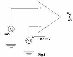
(A) 6000 (B) 5000
(C) 8000 (D) 9000
j. In the fabrication of integrated resistors, the sheet resistance of the base diffusion will be typically
(A)
![]() (B)
(B)
![]()
(C) ![]() (D)
(D)
![]()
Answer any FIVE Questions out of EIGHT Questions.
Each question carries 16 marks.
Q.2 a. Are passive components as important as active components in an electronic circuit? Justify your answer with relevant comments. What do you mean by resistance of a material? What is its measuring unit? Briefly explain the construction of the metalised type of carbon composition resistors, with an illustration. (9)
b. What is a vaccum tube? Why semiconductor devices have not fully replaced vaccum tubes in electronic applications? Write four lines about a vaccum diode. (7)
Q.3 a. What is a semiconductor? Write two important properties of a semiconductor. Illustrate by neat sketches the crystal structure and energy-band diagram, for the generation of electron- hole pair in an intrinsic semiconductor at room temperature. (8)
b. Draw the circuit for drawing the V-I characteristics of a PN-junction diode and explain the procedure for obtaining the characteristic. (8)
Q.4 a. What is the region of operation of a Zener diode? Briefly explain the Zener effect. Draw the simplest zener-diode voltage regulator and briefly explain. (11)
b. What is a light emitting diode? What are the commonly used materials in the manufacture of LEDs? Draw the circuit symbol for an LED. (5)
Q.5 a. Draw the schematic of an NPN transistor biased for active operation, and explain the transistor action. (8)
b. In equation form write the relationship that exists between the output and input quantities of a BJT and an FET and comment on the nature of variation. (5)
c. The data sheet of an FET lists these typical values:
![]() and
and ![]() .
.
Calculate the drain
current for ![]() . (3)
. (3)
Q.6 a. Draw a simple block diagram of feedback amplifier. Distinguish between positive feedback and negative feedback. Mention the features of negative feedback. (7)
b. Illustrate the following basic ways of connecting the feedback signal in an amplifier, and make the illustrations self-explanatory:
i. Voltage-series feedback.
ii. Current-shunt feedback. (4) (8)
c. Draw
the circuit of a practical phase-shift oscillator using a JFET. If in the
feedback circuit of the above oscillator, the value of the resistance used is ![]() , find the value
of the capacitance for oscillator operation at 1KHz. (5)
, find the value
of the capacitance for oscillator operation at 1KHz. (5)
Q.7 a. Distinguish between an analog signal and a digital signal. Define the following logic operations and write their standard symbol.
(i) The AND logic
(ii) The OR logic
(iii) The NOT logic (8)
b. Represent the given Boolean function on K-map.
![]() (4)
(4)
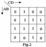
c. The K-map for a four-variable case is shown below in Fig.2. Write the simplified Boolean expression grouping the 1s. (4)
|
Q.8 a. What do you mean by a “logic family”? What are the main elements of a bipolar IC? What are the types of operations with bipolar ICs? Write the meaning of each one of the operations you mention. (8)
b. What do you mean by the following terms of digital ICs:
(i) Figure of merit
(ii) Noise margin. (4)
c. How is a CMOS obtained? Illustrate a CMOS switch by a neat sketch and mention its features. (4)
Q.9 a. What is an OPAMP? Distinguish between single-ended input operation and double-ended input operation. Define the quantity CMRR for an OPAMP. (8)
b. The
output voltage of an OPAMP with input voltages of 150 ![]() and 140
and 140![]() at its inputs is 40.006
mv. If
at its inputs is 40.006
mv. If ![]() for
the amplifier is 4000, compute the value of CMRR. (4)
for
the amplifier is 4000, compute the value of CMRR. (4)
c. Briefly explain the operation of a basic OPAMP integrator. (4)