DECEMBER 2006
Code: D-08 Subject: ANALOG ELECTRONICS
Time: 3 Hours Max. Marks: 100
NOTE: There are 9 Questions in all.
· Question 1 is compulsory and carries 20 marks. Answer to Q. 1. must be written in the space provided for it in the answer book supplied and nowhere else.
· Out of the remaining EIGHT Questions answer any FIVE Questions. Each question carries 16 marks.
· Any required data not explicitly given, may be suitably assumed and stated.
Q.1 Choose the correct or best alternative in the following: (2x10)
a. For a transistor to work as an amplifier the emitter base and base collector junctions are biased as follows:
(A) Both junctions are forward biased.
(B) Both junctions are reverse biased.
(C) Emitter base junction forward biased and collector base junction reverse biased.
(D)
Emitter base
junction reverse biased and collector base junction forward biased.
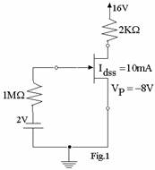
b. Calculate the voltage ![]() for
for
the circuit shown below in Fig.1:
(A) 16 volts.
(B) 4.75 volts.
(C) 0 volts.
(D) 2 volts.
c. The common base
current gain of a transistor ![]() . The common emitter current gain
. The common emitter current gain ![]() of the transistor
is:
of the transistor
is:
(A) 20. (B) 50.
(C) 49. (D) 100.
d. The voltage gain of a typical source follower amplifier is:
(A) 100. (B) 0.9.
(C) 1.1. (D) 0.5.
|
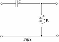
e. The circuit shown below in Fig.2 may be used as
(A) Low pass filter.
(B) High pass filter.
(C) Band pass filter.
(D) Band reject filter.
f. Tuned circuits are useful in amplifiers of the following class of operation.
(A) Class A (B) Class B
(C) Class C (D) Class AB
g. The maximum efficiency of a class B amplifier is likely to be:
(A) 100%. (B) 50%.
(C) 78%. (D) Around 75%.
|
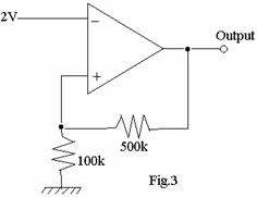
h. The output voltage of the amplifier
circuit shown below in Fig.3 is:
(A) 12 volts.
(B) 10 volts.
(C) 2 volts.
(D) 20 volts.
|
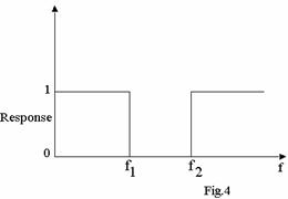
i. The frequency response of a circuit
is shown below in Fig.4. The name
of the circuit is
(A) Low pass filter.
(B) High pass filter.
(C) Band pass filter.
(D) Band reject filter.
j. The Barkhausen criteria for oscillation is stated as
(A) AB = 1. (B) A = 1.
(C) B = 1. (D)
AB ![]() 1.
1.
Answer any FIVE Questions out of EIGHT Questions.
Each question carries 16 marks.
Q.2 a. Compare the performance of common emitter, common base and common collector amplifier configuration. (8)
b. Draw the drain and transfer characteristics of n channel depletion mode MOSFET device. Explain the characteristic curves with the help of a circuit showing the voltages applied. (8)
Q.3 a. Draw the output characteristics of a common emitter connected transistor and explain the concept of cut off, active and saturation regions of a transistor. (6)
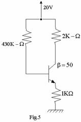
b. Calculate the collector current, and collector emitter voltage of the emitter stabilized circuit shown below in Fig.5. Make suitable assumptions and specify them if the given data is not sufficient. (10)
|
Q.4 a. What do you understand by Miller effect? Derive an equation to find the equivalent input capacitance due to Miller effect. (6)
b. Draw the frequency response of a JFET amplifier in any one of the configurations. Explain the various parameters that affect the low frequency and high frequency response of such an amplifier. (10)
Q.5 a. Explain operation of amplifier circuits by class A, class B, class AB and class C. (8)
b. Derive an equation for the maximum efficiency of a class B amplifier. Why it is less than 100 percent? (8)
Q.6 a. List out the specifications of an operational amplifier to be considered for the operation of an op amp circuit. (10)
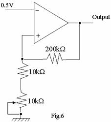
b. Calculate the range of output voltage
developed by the circuit shown bellow in Fig.6. (6)
Q.7 a. What is the response of a Butterworth Low Pass filter? Draw a second order Butterworth Low pass filter and explain its operation. (8)
b. Draw and explain the operation of a sample and hold circuit. (8)
Q.8 a. Draw and explain the circuit diagram of a phase shift oscillator using an op amp. What are the conditions for oscillation and what is the frequency of oscillation of such a circuit? (8)
b. What is piezo electric effect? (3)
c. Draw the electrical equivalent circuit of a quartz crystal which can be used as an oscillator. Explain how the properties of a crystal are used to generate electrical oscillations. (5)
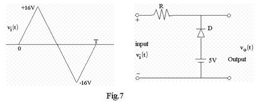
Q.9 a. Determine the output voltage for the circuit shown below in Fig.7. Assume ideal diode. (6)
 |
b. Draw the circuit diagram of a square wave generator using op amps and explain its operation. (10)