DECEMBER 2006
Code: D-06 Subject: BASIC ELECTRONICS
Time: 3 Hours Max. Marks: 100
NOTE: There are 9 Questions in all.
· Question 1 is compulsory and carries 20 marks. Answer to Q. 1. MUST BE WRITTEN IN THE SPACE PROVIDED FOR IT in the answer book supplied and nowhere else.
· Out of the remaining EIGHT Questions answer any FIVE Questions. Each question carries 16 marks.
· Any required data not explicitly given, may be suitably assumed and stated.
Q.1 Choose the correct or best alternative in the following: (2x10)
a. The colour band sequence of a resistor is grey, Blue, gold, and gold. The range in which its value must lie so as to satisfy the tolerance specified is between
(A)
![]() and
and ![]() (B)
(B)
![]() and
and ![]()
(C)
![]() and
and ![]() (D)
(D)
![]() and
and ![]()
b. A device whose characteristics are very close to that of an ideal current source is
(A) A gas diode. (B) a BJT in CB mode.
(C) a BJT in CE mode. (D) a triode.
c. In an N-type semiconductor, the concentration of minority carriers mainly depends upon
(A) the doping technique. (B) the number of donor atoms.
(C) the temperature of the material (D) the quality of the intrinsic material,
Ge or Si.
d. When forward bias is applied to a junction diode, it
(A) increases the potential barrier.
(B) decreases the potential barrier.
(C) reduces the majority-carrier current to zero.
(D) reduces the minority-carrier current to zero.
e. The theoretical maximum efficiency of a Bridge rectifier circuit is
(A) 48.2%. (B) 81.2%.
(C) 82%. (D) 40.6%.
f. The input resistance of a common-collector configuration will be of the order of
(A)
![]() (B)
(B)
![]()
(C) ![]() (D)
(D)
![]() and
above
and
above
g. A switching voltage regulator can be of the following type:
(A) step-down (B) step-up
(C) inverting (D) none of these
h. A UJT contains
(A) four pn junctions (B) three pn junctions
(C) two pn junctions (D) one pn junction
i. The foundation on which an IC is built is called
(A) an insulator. (B) a base.
(C) a wafer. (D) a plate.
j. X-ray tubes make use of
(A) Thermionic emission. (B) Secondary emission.
(C) High field emission. (D) Photoelectric emission.
Answer any FIVE Questions out of EIGHT Questions.
Each question carries 16 marks.
Q.2 a. Why colour coding system is used to indicate the value of a resistor? What is the role of a capacitor in an electronic circuit? Write a brief note on paper capacitors. (8)
b. Illustrate and explain the V-I characteristic of a practical current source. Comment on the equivalence between voltage source and current source. (6)
c. A dc source of strength 6 volts is driving a load whose resistance varies from two to twenty ohms. Compute the variation in terminal voltage for the source as a percentage. Take the source resistance as two ohms. (2)
Q.3 a. What is a semiconductor? Give its important properties. Briefly explain the energy band diagram for a semiconductor. (10)
b. Define the following as applied to a PN-junction:
(i) Depletion region (ii) Width of the barrier
(iii) Barrier voltage (iv) Height of the barrier
Support your answer with neat illustrations. (6)
Q.4 a. A centre-tap
full-wave rectifier is supplying to a load of one kilo-ohm. If the voltage
across half the secondary winding of the input transformer is 220 sin![]() , calculate the
following:
, calculate the
following:
(i) the peak value of current (ii) the r.m.s. value of current
(iii) the average value of the current (iv) the ripple factor
(v) the efficiency of rectification
For the diodes used assume each having their forward resistance is 10 ohms. (10)
b. A half-wave rectifier has a peak output voltage of 12.2V at 50 hertz and feeds a resistive load of 100 ohms. Determine the value of the shunt capacitor to give one percent ripple factor and the dc voltage output. (6)
Q.5 a. What do you mean by a voltage regulator? Distinguish between a linear regulator and a switching regulator. Draw the circuit of a simple emitter-follower regulator and briefly explain. (12)
b. What are the unique features of IC voltage regulators? (4)
Q.6 a. How are BJTs classified? Draw the circuit symbol for each type. What are the advantages of transistors over electron tubes? (8)
b. A transistor has an alpha dc of 0.98 and a collector leakage current of one microampere. If the emitter current is one milliampere, find the magnitude of the collector and the base currents. (4)
c. Give a table of comparison between CE and CB configurations with regard to the important parameters. (4)
Q.7 a. How does an FET differ from the conventional junction transistor? In the structure of an N-channel JFET, why the N-type bar is called a channel? Give the structure of a P-channel JFET. What is the difference between a JFET and a MOSFET? (9)
b. Write a brief note on DIAC. (7)
Q.8 a. What is an OPAMP? Why is it called so? Briefly explain the following for an OPAMP
(i) Input offset voltage (ii) Input bias current
(iii) CMRR (9)
b. Give the circuit of a popular inverting voltage amplifier using an OPAMP and derive the equation for the closed loop gain of the amplifier. (4)
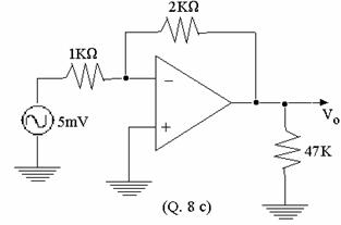
c. For the circuit shown calculate the following:
(i) the closed loop voltage gain.
(ii) the feedback fraction and
(iii) the closed-loop input impedance seen by the a.c. source. (3)
Q.9 a. Briefly explain the following methods of electron emission:
(i) Secondary emission (ii) Photoelectric emission (6)
b. Briefly describe the two types of etching commonly used in IC fabrication. (6)
c. Write a note on varactor. (4)