DECEMBER 2006
Code: C-03 / T-03 Subject: BASIC ELECTRONICS & DIGITAL CIRCUITS
Time: 3 Hours Max. Marks: 100
NOTE: There are 9 Questions in all.
· Question 1 is compulsory and carries 20 marks. Answer to Q. 1. must be written in the space provided for it in the answer book supplied and nowhere else.
· Out of the remaining EIGHT Questions answer any FIVE Questions. Each question carries 16 marks.
· Any required data not explicitly given, may be suitably assumed and stated.
Q.1 A. Choose the correct or best alternative in the following: (2x10)
a. When a reverse bias is applied to a junction diode, it
(A) lowers the potential barrier.
(B) increases the potential barrier.
(C) greatly increases the minority-carrier current.
(D) greatly increases the majority-carrier current.
b. Hall effect was discovered by Hall in
(A) 1800 (B) 1820
(C) 1874 (D) 1890
c. In a CB configuration the output characteristics of the transistor will be described by the plots of
(A)
![]() versus
versus ![]() for constant
for constant ![]() .
.
(B)
![]() versus
versus ![]() for constant
for constant ![]() .
.
(C)
![]() versus
versus ![]() for constant
for constant ![]() .
.
(D)
![]() versus
versus ![]() for constant
for constant ![]() .
.
d. The CE amplifier, when compared to a CB amplifier, has
(A) lower input resistance. (B) higher output resistance.
(C) lower current amplification. (D) higher current amplification.
e. The emitter
resistor ![]() when
bypassed by a capacitor
when
bypassed by a capacitor
(A) reduces the voltage gain. (B) increases the voltage gain.
(C) causes thermal runaway. (D) stabilises the ‘Q’ point.
f. The binary stream 100110010 in hexa-decimal system is
(A)
![]() (B)
(B) ![]()
(C) ![]() (D)
(D)
![]()
g. The
simplified expression for the function ![]() is
is
(A)
![]() (B)
(B) ![]()
(C) ![]() (D)
(D)
![]()
h. For high speed TTL, propagation delay in nanoseconds is, approximately
(A) 10 (B) 8
(C) 6 (D) 15
i. The
number of flip-flops required for a counter that will count 0 to ![]() is
is
(A) Four (B) Six
(C) Eight (D) Sixteen
j. Karnaugh map simplifies Boolean functions based on the following Boolean identity
(A) A.1 = A (B)
A+![]() =1
=1
(C) A+0 = A (D) A+1 =1
Answer any FIVE Questions out of EIGHT Questions.
Each question carries 16 marks.
Q.2 a. What is an extrinsic semiconductor? Name the different types of extrinsic semiconductors. What is Hall effect and what is its use in semiconductors? (7)
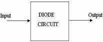
b. A sinusoidal signal is applied to a diode
circuit shown to get the output as indicated. Draw two circuits which use a
single diode and which generates the same output waveform.
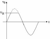
Assume
that the Peak of the input voltage is greater than ![]() . (4)
. (4)
c. What is a Bipolar junction transistor? Write the circuit symbol of a bipolar junction transistor. Briefly explain the output characteristics of a CE configuration. (5)
Q.3 a. What are the important parameters of an amplifier? Define each one of them. Draw the hybrid-model of a CB amplifier and define the various hybrid parameters of the model. (11)
b. Write a brief note on Darlington pair. (5)
Q.4 a. Write the importance of source, Drain, Gate and Chanel in a JFET. (7)
b. What is a crystal oscillator? For what applications do you recommend crystal oscillators? Draw the circuit of a pierce crystal oscillator using FET and mention its features. (9)
Q.5 a. A center-tapped fullwave rectifier circuit uses a transformer having a turns ratio of 0.2 and employs a load of 100 ohms. If the circuit is driven by a single phase 230V, 50Hz power supply, calculate
(i) the d.c. output voltage
(ii) the PIV of the diodes and
(iii) the rectification efficiency.
Assume the diodes to be ideal. (6)
b. Draw the circuit of a basic differentiator using an OPAMP and explain its operation. (5)
c. What do you mean by a regulated power supply? What are the important elements of a regulated power supply? Define the term voltage regulation. (5)
Q.6 a. Express the Boolean function, ![]() in a product of sums
form. (5)
in a product of sums
form. (5)
b. Simplify the Boolean
function ![]() using K-Map.
using K-Map.
![]() (4)
(4)
c. What is a ROM? What is its advantage? Write the block diagram of a ROM and briefly explain. (7)
Q.7 a. A Bipolar
junction transistor in common emitter configuration is biased at a quiescent collector
current ![]() of 1 mA. It is known that the
transistor will just enter saturation region if the collector current becomes
1.617 mA. Determine the change in
of 1 mA. It is known that the
transistor will just enter saturation region if the collector current becomes
1.617 mA. Determine the change in ![]() of the transistor from its quiescent
value such that it just enters saturation. (8)
of the transistor from its quiescent
value such that it just enters saturation. (8)
b. What is a Schottky diode? What are its advantages? Draw the circuit of a CMOS NOR gate and briefly explain. (8)
Q.8 a. Draw the circuit of a TTL NAND gate with totem pole output and briefly explain. (8)
b. Write a note on EPROM. (8)
Q.9 a. What do you mean by ‘clocked sequential circuits’? Draw the circuit of a clocked D flip-flop that uses only NAND gates and briefly explain its working. (8)
b. What is a synchronous binary counter? Draw the schematic of a 4-bit synchronous binary counter using JK flip-flops and briefly explain its operation. (8)