DECEMBER 2006
Code: A-27 Subject: DIGITAL HARDWARE DESIGN
Time: 3 Hours Max. Marks: 100
NOTE: There are 9 Questions in all.
· Question 1 is compulsory and carries 20 marks. Answer to Q. 1. must be written in the space provided for it in the answer book supplied and nowhere else.
· Out of the remaining EIGHT Questions answer any FIVE Questions. Each question carries 16 marks.
· Any required data not explicitly given, may be suitably assumed and stated.
Q.1 Choose the correct or best alternative in the following: (2x10)
a. In VHDL, a package declaration is used to
(A) Bind architecture body to its entity declaration
(B) Store a set of common declarations, such as components, types, procedures, functions
(C) Support mixed style of modeling
(D) All of the above
b. In VHDL, a valid process statement consists of
(A) Both sensitivity list and wait statement
(B) Neither sensitivity list nor wait statement
(C) Either sensitivity list or wait statement
(D) A component instantiation statement
c. Which of the following statement is true with respect to moore/mealy machine
(A) In mealy machine the output is function of present state and external inputs.
(B) In moore machine the output is function of present state and external inputs.
(C) In mealy machine the output is function of only present states.
(D) In moore machine the output is function of only external inputs.
d. The correct answer of the simplified form of the Boolean equation
E1 (x2,x1,x0) = x2x1 + x2 x1’ + x2x0 is
E1(a, b, c) = ab+ab’+ac
(A) ab (B) ac
(C) b (D) c
e. A PROM has
(A) A hardwired AND array and a programmable OR array
(B) A hardwired OR array and a programmable AND array
(C) A programmable AND array and a programmable OR array
(D) A hardwired AND array and a hardwired OR array
f. When network is implemented by a 2k- input decoder using k-input decoder modules and two-input AND gates, decoder modules required by a coincident and tree decoder respectively are
(A) 2k +1 and 2k (B) 2 and 2k +1
(C) 22k and 2 (D) 2 and 22k
g. The circuit shown in Fig. 1 detects the following sequence
|
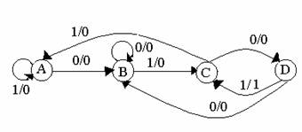
(A) 0001 (B) 0111
(C) 0101 (D) 1111
h. Hazards have serious effects in
(A) Synchronous sequential circuits
(B) Combinational circuits
(C) Asynchronous sequential circuits
(D) None of the above
i. The frequency of the clock generated by the statement CLK<=not CLK after 50 ns is
(A) 1 MHz (B) 10 MHz
(C) 100 MHz (D) 0.2 MHz
j. There is a D flipflop with its ![]() output and D input tied
together. Frequency of the output Q is equal to
output and D input tied
together. Frequency of the output Q is equal to
(A) same as the input frequency (B) half of the input frequency
(C) double the input frequency (D) output Q always remains high
Answer any FIVE Questions out of EIGHT Questions.
Each question carries 16 marks.
Q.2 a. Generate the set of prime implicants and obtain all minimal expressions for the following function:
f(v,w,x,y,z)=∑(13,15,17,18,19,20,21,23,25,27,29,31) + ![]() (1,2,12,24) (9)
(1,2,12,24) (9)
b. Realize the given function using a single threshold gate.
F= CD + A’D + B’D + A’B’C (7)
Q.3 a. Define the following terms:
(i) FPGA
(ii) Digital systems
(iii) A modulo-P Counter
(iv) P- shifter
(v) Programmable sequential arrays
(vi) Configuration declaration in VHDL (6)
b. Implement one-bit full adder using 4- input multiplexers and discrete gates. (5)
c. Implement the sequential system shown in Table 1 by using a ROM. (The combination x1x0 =00 never appears, so consider it as a don’t care case.) (5)
|
PS |
x1 xO |
|
FFFFFF y1 y0 |
01 10 11 |
|
0 0 |
01,0 10,1 10,0 |
|
0 1 |
00,0 11,1 11,0 |
|
1 0 |
11,0 10,0 00,1 |
|
1 1 |
10,0 00,0 11,1 |
|
y1 y0, Z NS, Output |
Where PS is Present state and NS is Next state.
Q.4 a. Discuss how an incompletely specified machine can be simplified. (6)
b. A synchronous sequential circuit which produces an output pulse z =1, whenever the sequence 01101 occurs at the input is to be designed. Overlapping sequences are accepted. For example, if the input is 0101101101…, the required output is 0000001001…for the above,
(i) Draw a state diagram.
(ii) Select an assignment and show the excitation table and the output table.
(iii) Write down the excitation functions for T flip-flops and draw the corresponding logic diagram. (10)
Q.5 a. Discuss Linear separability of threshold functions. (5)
b. For the machine shown in Table 2, find the equivalence partition and the corresponding reduced machine in the standard form. (7)
|
PS |
NS, Z |
|
x=0 x=1 |
|
|
A |
E,0 C,0 |
|
B |
C,0 A,0 |
|
C |
B,0 G,0 |
|
D |
G,0 A,0 |
|
E |
F,1 B,0 |
|
F |
E,0 D,0 |
|
G |
D,0 G,0 |
Table 2
c. What do you understand by microinstruction sequencing? How explicit microinstruction sequencing is different from the implicit one? (4)
Q.6 a. Draw the state diagram and the state table of a serial adder as a
(i) Mealy machine.
(ii) Moore machine. (8)
b. First draw the ASM chart of a serial adder and then synthesize the circuit. (8)
Q.7 Write the VHDL code for the following:
(i) A combinatorial circuit that has two inputs a and b, one output y and two select lines S1 and S0. Depending upon the status of select lines, the output of the circuit is AND, OR, NOR. or NAND of the two inputs namely a and b.
(ii) 8 : 1 multiplexer
(iii) 4 : 16 decoder
(iv) Half adder using data flow style of modelling (16)
Q.8 a. Discuss the basic characteristics of fundamental mode ASM. A fundamental mode
asynchronous sequential machine has two inputs x1, x2 and two outputs z1, z2. The output Zi (i=1 or 2) assumes high logic level whenever the input that changed last was xi and 0 at all other times for the above.
(i) Draw the flow table.
(ii) Select the valid assignments and synthesise the circuit. (12)
b. What are asynchronous circuits? What design features must be added to then so that they become hazard free? Discuss with the help of an example. (4)
Q.9 Write explanatory notes on (any FOUR)
(i) Behavioural style of modelling in VHDL
(ii) Priority encoders
(iii) Designing of digital circuits with and without CAD tools
(iv) FPLA
(v) Comparison of GAL and PAL devices. (4 x 4 = 16)