DECEMBER 2006
Code: A-05 Subject: BASIC ELECTRONICS
Time: 3 Hours Max. Marks: 100
NOTE: There are 9 Questions in all.
· Question 1 is compulsory and carries 20 marks. Answer to Q. 1. must be written in the space provided for it in the answer book supplied and nowhere else.
· Out of the remaining EIGHT Questions answer any FIVE Questions. Each question carries 16 marks.
· Any required data not explicitly given, may be suitably assumed and stated.
Q.1 Choose the correct or best alternative in the following: (2x10)
a. When the temperature of a doped semiconductor is increased, its conductivity
(A) decreases.
(B) increases.
(C) does not change.
(D) increases or decreases depending on whether it is p- or n-type.
b. The main characteristics of a Darlington Amplifier are
(A) High input impedance, high output impedance and high current gain.
(B) Low input impedance, low output impedance and low voltage gain.
(C) High input impedance, low output impedance and high current gain.
(D) Low input impedance, low output impedance and high current gain.
c. The
transconductance, ![]() , of a JFET is computed at constant
, of a JFET is computed at constant ![]() , by the following:
, by the following:
(A)
![]() (B)
(B)
![]() .
.
(C)
![]() . (D)
. (D) ![]() .
.
d. The feedback
factor ![]() at
the frequency of oscillation of a Wien bridge oscillator is
at
the frequency of oscillation of a Wien bridge oscillator is
(A)
3 (B)
![]()
(C) ![]() (D)
(D)
![]()
e. In an amplifier with negative feedback, the bandwidth is
(A)
increased
by a factor of ![]()
(B)
decreased
by a factor of ![]()
(C)
increased
by a factor of (1+A![]() )
)
(D) not affected at all by the feedback
where A = gain of the basic amplifier and
![]() = feedback factor.
= feedback factor.
f. The ‘slew rate’ of an operational amplifier indicates
(A) how fast its output current can change
(B) how fast its output impedance can change
(C) how fast its output power can change
(D) how fast its output voltage can change
when a step input signal is given.
g. In a clamping circuit, the peak-to-peak voltage of the waveform being clamped is
(A) affected by the clamping
(B) not affected by the clamping
(C) determined by the clamping voltage value
(D) determined by the ratio of rms voltage of the waveform and the clamping voltage
h. Regulation of a d.c. power supply is given by
(A) product of no-load output voltage and full-load current
(B) ratio of full-load output voltage and full-load current
(C) change in output voltage from no-load to full-load
(D) change in output impedance from no-load to full-load
i. A ‘literal’ in Boolean Algebra means
(A) a variable in its uncomplemented form only
(B) a variable ORed with its complement
(C) a variable in its complemented form only
(D) a variable in its complemented or uncomplemented form
j. In an unclocked R-S flip-flop made of NOR gates, the forbidden input condition is
(A) R=0, S=0 (B) R=1, S=0
(C) R=0, S=1 (D) R=1, S=1
Answer any FIVE Questions out of EIGHT Questions.
Each question carries 16 marks.
Q.2 a. What is ‘doping’ of a semiconductor? Explain how p- and n-type semiconductors are formed. Also write their energy band diagrams, clearly showing the different energy levels. (8)
b. What is Early effect? Explain how it affects the characteristics of BJT in CB configuration. (8)
Q.3 a. Draw a neat circuit of a differential amplifier and explain its operation. (10)
b. In a transformer, give the relationship between
(i) turns ratio and its primary and secondary impedances
(ii) turns ratio and primary/secondary voltage.
In a transformer-coupled
amplifier, the transformer used has a turns ratio N1:N2=10:1. If the source
impedance is 8 ![]() what
should be the value of load impedance for maximum power transfer to the load?
Also find the load voltage if the source voltage is 10 volts. (6)
what
should be the value of load impedance for maximum power transfer to the load?
Also find the load voltage if the source voltage is 10 volts. (6)
Q.4 a. Explain the effect of temperature on a JFET. (8)
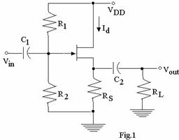
b. The FET circuit given
below in Fig.1, has ![]()
![]()
![]()
![]() and
and ![]() . Find its input impedance, output
impedance and voltage gain. (8)
. Find its input impedance, output
impedance and voltage gain. (8)
|
Q.5 a. State any four advantages of negative feedback in amplifiers. (5)
b. In an amplifier with negative feedback, the gain of the basic amplifier is 100 and it employs a feedback factor of 0.02. If the input signal is 40mV, determine
(i) voltage gain with feedback and
(ii) value of output voltage. (3)
c. Describe how oscillations are developed in a tank circuit. (8)
Q.6 a. Draw the circuit of a sample-and-hold circuit using op-amp. Explain its working with neat timing diagrams. (8)
b. Define the following terms as applied to characterization of op-amps
(i) CMRR (ii) slew rate (4)
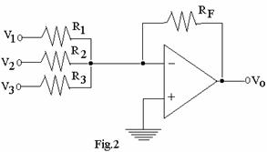
c. In
the circuit shown below in Fig.2, ![]() ,
, ![]() ,
, ![]() and
and ![]() . The inputs are:
. The inputs are: ![]() ,
, ![]() and
and ![]() . Compute the output
voltage. (4)
. Compute the output
voltage. (4)
|
Q.7 a. What are the different types of multivibrators? Briefly explain each type. (7)
b. Draw the circuit of an astable multivibrator using 555 timer. Derive the expression for its frequency of oscillation. (9)
Q.8 a. Draw a neat diagram to show the functional blocks of a complete regulated power supply. Explain the role of each block. (9)
b. A
half-wave rectifier has a load resistance of 3.5![]() . If the diode and secondary of the transformer
have a total resistance of 800
. If the diode and secondary of the transformer
have a total resistance of 800![]() and the ac input voltage has 240 V (peak
value), determine:
and the ac input voltage has 240 V (peak
value), determine:
(i) peak, rms and average values of current through load
(ii) dc power output
(iii) ac power input
(iv) rectification efficiency. (7)
Q.9 a. Draw the circuit of a 4-bit ring counter using suitable flip-flops. Explain its operation using timing diagrams and truth table. (8)
b. Show how a T-flop-flop can be constructed using J-K flip-flop. Write the truth table of T flip-flop. (2)
c. Implement AND, OR and NOT gates using
(i) NOR gates only (ii) NAND gates only (6)